 During the 80's the Department of Defense gave both Honeywell and Texas Instruments (TI) large classified contracts to develop uncooled infrared sensor technology. The military wanted a sensor that had very short turn-on time. Both programs were very successful - the pyroelectric sensor by TI and the microbolometer by Honeywell.
In 1992 the US Government de-classified the use of Infrared Technology for commercial products but maintained control of the technology. TI developed commercial imagers with their sensor technology and Honeywell licensed their microbolometer sensor technology to other companies.
Four companies originally purchased the microbolometer license. Loral, the company that purchased the Honeywell Electro Optics Division, received a license. Santa Barbara Research that was part of Hughes, Amber Engineering, and Rockwell purchased licenses. All four of these licenses have changed hands, some more than once. Loral was acquired by Lockheed Martin who later put the microbolometer activity in their Sanders operation which was later acquired by British Aerospace. Raytheon acquired Santa Barbara Research from Hughes and acquired Amber Engineering. Boeing acquired Rockwell's infrared activity and after a few years sold it to DRS Technologies. So the original four licensees are now three, British Aerospace, Raytheon and DRS Technologies.
Companies that currently have licenses to manufacture microbolometer arrays:
- Fluke Corporation
- BAE Systems
- Raytheon
- L-3 Communications Infrared Products
- DRS Technologies
- FLIR Systems
- InfraredVision Technologies Corporation
- NEC
- Institut National d’Optique (INO)
- Honeywell (Manufactured for Infrared Solutions)
- ULIS-IR
- SCD – SemiConductor devices
Microbolometer technology
Individual sensor elements use the change in electrical resistance of a VOx resistor deposited onto the tiny "platelets" fabricated by silicon micro-machining in a silicon foundry. Incoming target radiation heats the VOx causing a change in electrical resistance, which is readout by measuring the resulting change in current. 80,000 and more sensors can be fabricated together into a two-dimensional array. The structure can be dimensioned to operate at 30 Hertz. That is, the thermal conductance of the isolating legs can be adjusted to match the time-constant for 30-hertz operation. An example of a microbolometer element is pictured below.
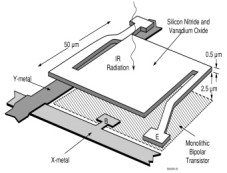
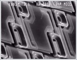
It consists of a two-layer structure. An interconnecting readout circuitry is applied to the silicon process wafer and then the microbolometer structure is built on top of the readout circuitry. First a pattern of islands _ wavelength thick are deposited on the readout circuitry. The islands are made of a material that can be selectively etched away later to form a bridge structure. Three layers -- silicon nitride, vanadium oxide, and silicon nitride -- are deposited over the sacrificial islands. The sacrificial islands are then etched away leaving the thermally isolated bridge structure of vanadium oxide. A photo of an early Honeywell microbolometer element is shown in the picture below followed by a photo of one corner of a 320 by 240 microbolometer array.
 Most of today's camera manufacturers use the 320 by 240 microbolometer array. However there is an excellent alternative for many commercial applications - the 160 by 120 array. The smaller array and its resulting camera can be produced at a much lower cost. Far more arrays can be produced on a single wafer and the yield is higher for the smaller array. In addition, one of the most expensive components of an infrared camera is the lens and its cost is proportional to the array size.
 The only advantage of the larger array is field of view (FOV). With the same f# and focal length lens and the same detector size, a camera with 320 by 240 or 160 by 120 will have identical spatial resolution. But the target size for a fixed distance between the camera and target will be twice as large in both dimensions for the camera with the larger array. For many commercial applications the cost savings of the smaller array size over shadows the advantage of a larger FOV.
It consists of a two-layer structure. An interconnecting readout circuitry is applied to the silicon process wafer and then the microbolometer structure is built on top of the readout circuitry. First a pattern of islands _ wavelength thick are deposited on the readout circuitry. The islands are made of a material that can be selectively etched away later to form a bridge structure. Three layers -- silicon nitride, vanadium oxide, and silicon nitride -- are deposited over the sacrificial islands. The sacrificial islands are then etched away leaving the thermally isolated bridge structure of vanadium oxide. A photo of an early Honeywell microbolometer element is shown in the picture below followed by a photo of one corner of a 320 by 240 microbolometer array.
Most of today's camera manufacturers use the 320 by 240 microbolometer array. However there is an excellent alternative for many commercial applications - the 160 by 120 array. The smaller array and its resulting camera can be produced at a much lower cost. Far more arrays can be produced on a single wafer and the yield is higher for the smaller array. In addition, one of the most expensive components of an infrared camera is the lens and its cost is proportional to the array size. The only advantage of the larger array is field of view (FOV). With the same f# and focal length lens and the same detector size, a camera with 320 by 240 or 160 by 120 will have identical spatial resolution. But the target size for a fixed distance between the camera and target will be twice as large in both dimensions for the camera with the larger array. For many commercial applications the cost savings of the smaller array size over shadows the advantage of a larger FOV.
VOx technology
The superior IR detection technology
Infrared Solutions, Inc. combines the world’s most sensitive uncooled IR detector material with proprietary Read Out Integrated Circuitry, designed to optimize image quality in its infrared cameras. Other uncooled sensor materials used in competitive IR cameras do not possess the high levels of thermal sensitivity and accuracy of VOx.
Infrared Solutions, Inc. combines the world’s most sensitive uncooled IR detector material with proprietary Read Out Integrated Circuitry, designed to optimize image quality in its infrared cameras. Other uncooled sensor materials used in competitive IR cameras do not possess the high levels of thermal sensitivity and accuracy of VOx.

- Long wavelength, 8-14μm operational spectrum is the most efficient radiation transmission band
- Immune to “sun glints”— false positives that plague short wave-band IR cameras
- Provides greater sensitivity at the most encountered temperature conditions
- Proprietary Infrared Solutions Read Out Integrated Circuitry (ROIC) allows for greater thermal sensitivity
- Superior thermal sensitivity compared to other materials used in other IR sensors
- Delivers finer pixel pitch, greater spatial resolution and smaller package sizes
- The VOx microbolometer is export controlled by the Department of Defense due to it’s advanced thermal sensitivity
- Made in the USA